We are currently working on an updated version of the PRO PCB with these main changes:
- Migration to KiCad
- Added ground plane
- Improved tracings
Gerber and KiCad files: public – Google Drive
Please provide feedback if you have any.
We are currently working on an updated version of the PRO PCB with these main changes:
Gerber and KiCad files: public – Google Drive
Please provide feedback if you have any.
Are the black rectangles cut outs (holes) for cable ties around components? If so, I already love it. That has been a major issue for me with my v3.3.
Do I understand correctly that the new tracings and the additional ground plane might resolve some of the i2c instabilities? Changing the i2c speed helped me to improve communication stability somewhat, so I wonder if the latest changes might address the root cause. Great job, folks! 
Yes, the black holes are for zip ties and the larger ones are large cutouts (to reduce the temperature impact from the board on the temperature sensor).
By the way, this is also why the ground plane does not reach completely to the temperature sensor.
There seems to be a bundle of different issues impacting the i2c stability. @ken830 and others did some great work on this, so it’s difficult to say what extend these changes have.
Are you running the AirGradient software or ESPHome?
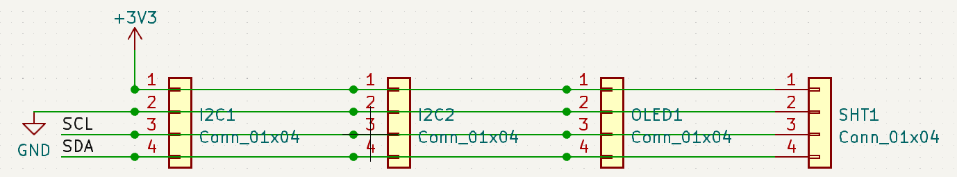
Schematics are mostly a style preference, but it’s never a good idea to draw your wires across symbols. Schematic entry tools also behave funny with overlapping nets and pins and you could have rogue nets hidden underneath things that can come back to haunt you later.
For example, the I2C headers have wires that run right over them:
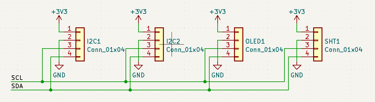
Something like this would avoid potential problems and still be easy to read:
For the layout, were there any thoughts on moving to a 4-layer PCB? With a 2-layer, you’re essentially getting the same general layout as previous boards with the added broken-up ground fill.
I’m still not 100% convinced on what and by how much needs to be improved. The LDO on my D1 Mini seems to have failed while I was probing around, so I haven’t been able to complete my investigation yet. I have a few D1 Mini clones coming from Amazon hopefully in a week or so. AliExpress and the official Wemos stuff would take much longer to get.
What’s the D1 Mini Shield part for? To support shields? Would it be possible to use long header pins to stack the shield with the D1 Mini and save a lot of routing space on the PCB?
I am running esphome. I am not a big fan of the subscription trend everywhere, although I understand it’s sometimes unavoidable. I saw the “includes 12 months of using our AirGradient software” and thought I’d rather avoid another subscription.
Speaking of that, I really enjoyed the newsletter today/yesterday, where you commented on the topic. Much appreciated thoughts. It made me feel like giving the AirGradient software a try sometime, and I am happy to be a part of this community. Off-topic, back to the new board design!
can you run the Schematics out as PDF. I don’t have the time to install and learn KiCad
In my life (and I’m not even layout engineer), I have had to use DipTrace, Eagle, Altium, CadStar, CR-5000 and Mentor BoardStation - I’m not about to start using another tool
The Gerbers I can see in gerbv and ViewMate
Layout comments:
Here is a link to the schematics as pdf: https://drive.google.com/file/d/1tRGaRt2bbshd5wQ02PUusfOD7bTWvoW0/view?usp=share_link
We tested this extensively on our commercial monitor and the copper plate has a noticable effect in heat transfer to the temperature sensor.
Yes, the idea is to support shields. The shields could theoretically put on top of the D1 but then it might get too tall for the enclosure.
Personally I would add a decoupling cap at the 5V to the CO2 sensor and the 3.3V at the display.
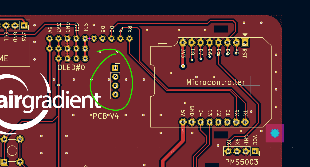
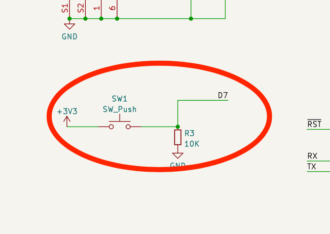
What is this switch putting 3V straight into D7 (MOSI) - here I would put a 1kOhm in series
Definitely agree with Ken’s comment on the Schematic there.
I just realized the other day that I was mistaken. All along, I thought the OLED was powered by 5V, not 3.3V. I would strongly advocate for powering the OLED with 5V and taking the load off the LDO which might already be close to or at its current delivery limit. Because we don’t know what LDO comes with clones, it’s better to power move as much as we can to 5V.
I agree with l4ur’s concerns regarding the button. I don’t know the start-up conditions, but if you can, reverse the logical polarity of that input and just pull-up to +3.3V. Then the switch can shunt it to ground when pressed. Doesn’t add an extra component and it’s safer.
Assuming clean, within-specs USB power source, I don’t think the S8 needs any decoupling on the PCB. The S8 has internal 3.3V voltage regulators and will have it’s own set of filtering and decoupling.
I can see a path to really clean routing without the shield headers even with only 2 layers.
@ken830 Are you sure having i2c for the OLED on 5v will not impact the communication as the D1 i2c works on 3.3v and could have any unwanted implications.
Regarding the other discussion, we plan to change the following:
There are only 2 points of interaction between the OLED and the microcontroller: SCL and SDA. I2C is a shared open-drain bus and the only possible interactions with the bus is to pull it low or sample its voltage, which is defined by the pull-up resistors and the voltage they are tied to. Powering the OLED with 5V or 3.3V shouldn’t make any difference in the I2C interface because the OLED has an onboard LDO that generates 3.3V which it uses to pull up the I2C lines.
If anything, it’s probably slightly better for the I2C interface to power with 5V because we don’t know the specs of the onboard LDO and all LDOs have a minimum dropout voltage – in fact, LDO = Low DropOut Regulator. That means if we power the OLED with 3.3V, the onboard LDO will likely be regulating that down to 3.2V or lower and pull the I2C bus to that slightly-lower voltage instead, slightly slowing the apparent rise times and slightly lowering your VIH margins… If you buy these OLED in large enough quantities, perhaps we could get schematics or specifications?
Since I now have two PCBs with both configurations (3.3V and 5V), I could take some measurements, but the v3.7 pre-assembled board has tape covering the backside of the OLED and it’s soldered down. I’ll have to cut away part of the tape to get to the LDO output…
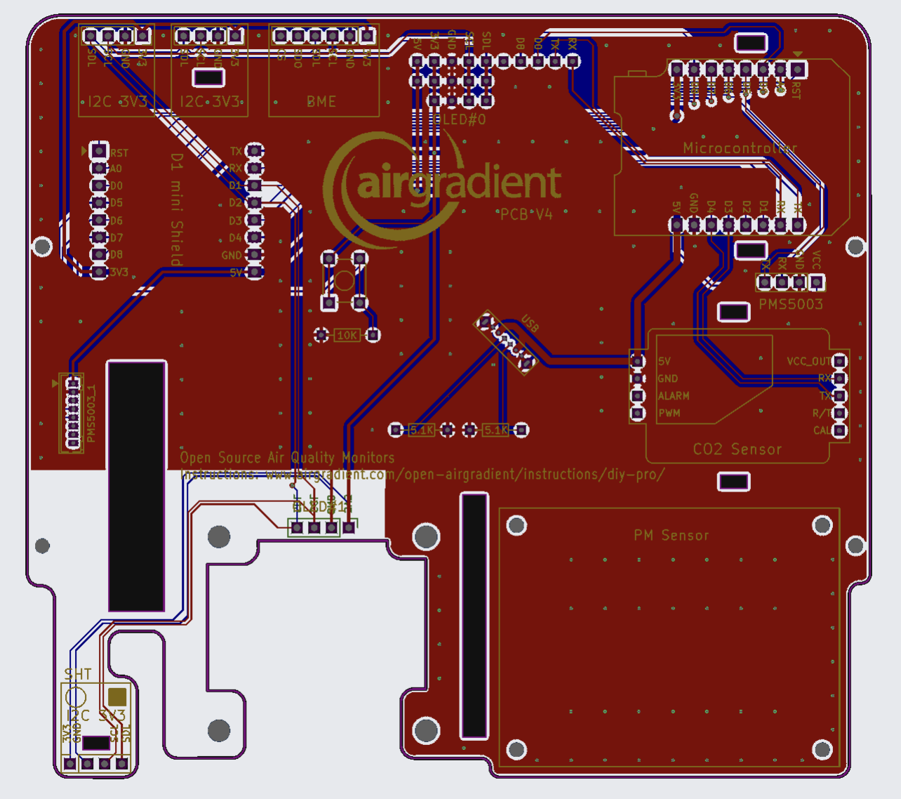
Is it possible to get rid of the 4-pin PMS5003 connector, move the 8-pin to that location, and get a shorter JST cable? That would also simplify the routing by quite a bit. Or if we need to maintain the 4-pin for people to solder wire leads, then maybe squeeze the two connectors right next to each other – I assume you will use one or the other, never both.
@ken830 Thank you for clarifying the OLED i2c with 5v.
I would like to maintain the 4 pin throughole for the people that are not proficient in soldering the small pins. We often run workshops with young students and these small pins are challenging for them to solder.
The PMS cable comes with the PMS sensors and the supplier has only this cable available. Thus we would like to use it and not discard it. So the location of the current JST pin has been selected due to the cable length. Do you see any functional problem with the current location of the plug?
Out of curiosity (and as somebody who is not an electronics expert), what are the expected benefits to this new Pro PCB version for end-users?
I skimmed through https://forum.airgradient.com/t/design-flaw-of-all-airgradient-pcbs/, and it seems like this will help improve the reliability somehow, of the readings - is that correct?
And the mentions of cable routing here - I assume that will make the internal layout and cables a bit neater, and easier to diagnose, right?
@Achim_AirGradient : Understood. I think keeping the 4-pin is fine, but moving the 8-pin JST next to it is going to be very beneficial in terms of better routing on the PCB and reducing the total length of the signal path. Since we’re removing the shield breakout, there’s no longer a reason to run the traces to that side of the PCB anymore. The same goes for the 5V rail. It would no longer have to run to that side of the board, which will simplify routing and give you a more solid ground plane. It should be okay to just fold-over the long cable a few times (and maybe zip-tie it) to prevent it from flopping around.
Can you also elaborate on what the the Ext connector is and what the extra rows of pins are. I can kind of guess for OLED #0, but not entirely sure. Are you trying to support some legacy configurations?
Also, if you add some through-hole (not nearly as good as surface mount, but keeps it DIY-friendly) capacitors at each of the module’s power pins, we can decide later if they are needed or not, but having a footprint there will keep the option available.
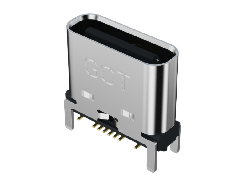
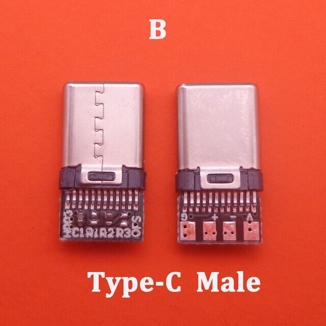
I’ve been thinking about the USB Type-C connector a lot. It would be very nice to get a data connection so that we don’t have to take apart the case to re-program the D1 Mini. Unfortunately, I was not able to find a vertical USB Type-C connector with the data pins that is through-hole. The closest I could find is this one: https://gct.co/connector/usb4145
Unlike most surface-mount connectors, it has surface-mount leads that protrude out the side making it feasible for hand-assembly. Obviously, it will still be more difficult compared to the current through-hole-only connector. Another thing is the height profile is only 7.46mm compared to the ~10.5mm profile of the current connector. This means that it won’t protrude far enough to make plugging in cables possible with the case on. I think to solve both of these problems, we could add this secondary connector and located it in the center of the larger hole in the case. That means it would be optional and the larger hole will allow plugging in the cable without interference from the case.
With the Dp and Dn data pins on this secondary connector, we can figure out how to connect that to the D1 Mini. At first, I though a header, but I couldn’t find a simple USB Type-C to header cable. Then, I thought we could find a USB-C Male connector breakout board with 0.1" pin pitch spacing, but I couldn’t find anything. This one would be perfect, but it’s a female receptacle:
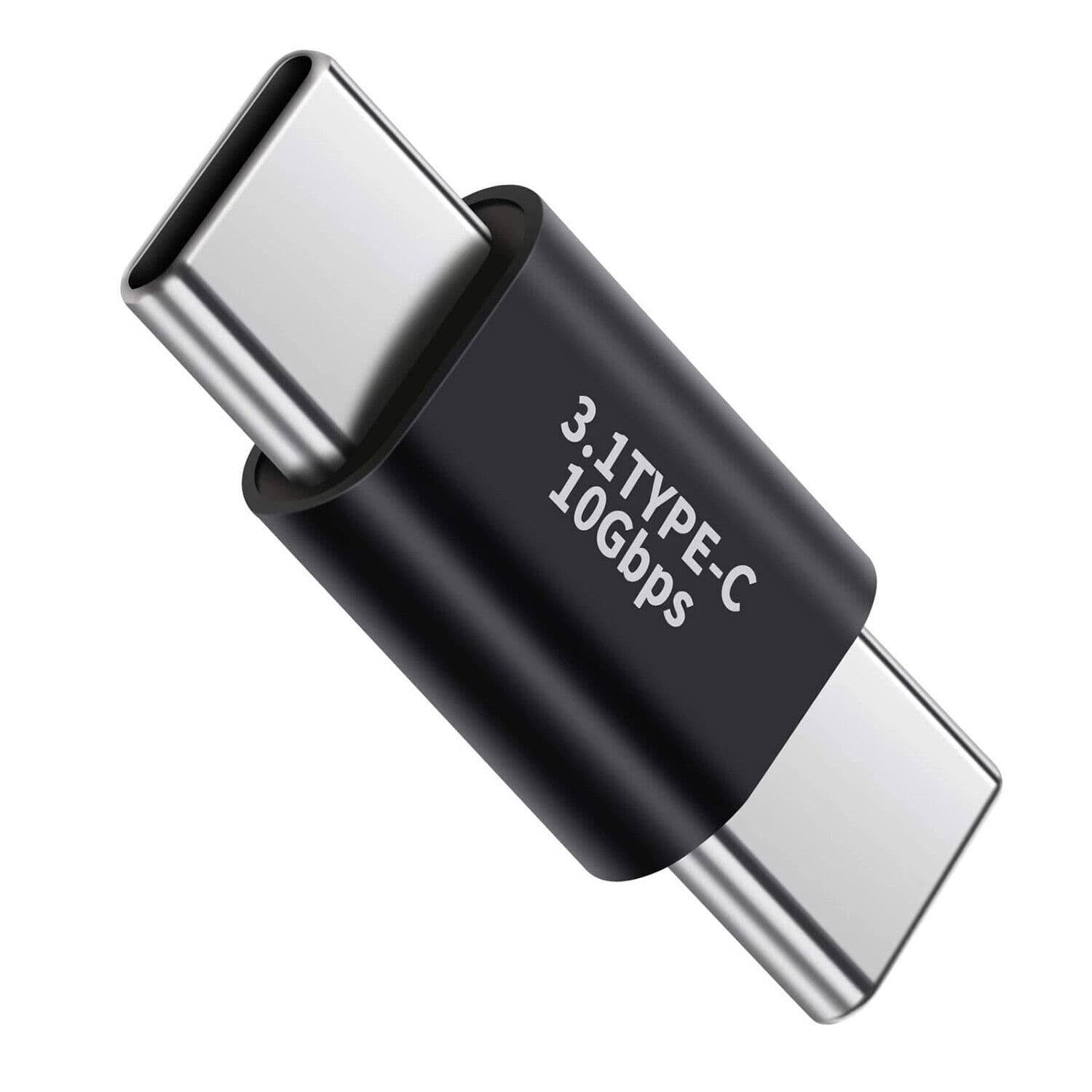
Perhaps we could still use this along with a male-to-male adapter (something like this):
But the problem is the length of the adapter would affect where the header is located on the PCB. I guess the easiest would be to just use a male breakout like one of these and just wire up to a header on the PCB:
Another option is to design our own breakout board – a small PCB with a USB C male connector and a spot to solder in header pins that will match the header on the PCB. We could use the space where the OLED cutout is, and just have it snap off, so it won’t cost any extra to manufacture and will give people an option. I understand this is a bit more complex logistically, though.
It would look something like this:
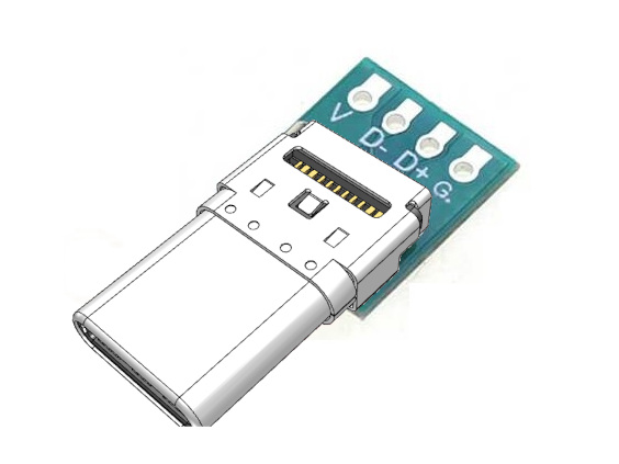
On the PCB, the extra header will look something like this:
@victorhooi Others may have a different opinion, but I don’t think the reliability of the current design is a problem. I’ve worked through the rebooting issue (exception 0 crash caused by a breaking change in the SoftwareSerial library v7) and the serial timeout issue (caused by a bug in an older version of SoftwareSerial library). The I2C instability is likely because of the slow rise times that are MUCH too slow for operating at I2C fast mode (400kHz). I gave instructions on how to set this to standard mode (100kHz). The rise time is plenty fast for standard mode and there’s no down-side. I’ve analyzed the power at the SGP sensor based on concerns raised in that thread and it looks acceptable to me. The 3.3V LDO regulator on the D1 Mini clone PCBs may be undersized for our application, but that’s not clear since we don’t have exact part number to look up the specs. That will be improved if this new version of the PCB moves the OLED over to the 5V rail.
The breakouts at the top are for custom extensions of the board and OLED#0 in case somebody want to plug in an OLED display for debugging purposes (then no need to turn the board around all the time).
Regarding the USB plug, I think it’s important to keep the design clean and simple. For temporary debugging, one could plug in the cable into the D1 and then lead it through the square cutout in the enclosure to the outside,
If we use the ESP32-C3 module in the future, it will be easier to feed out the debug signal and flash it through the standard USB plug (we designed it that way on the outdoor kit).