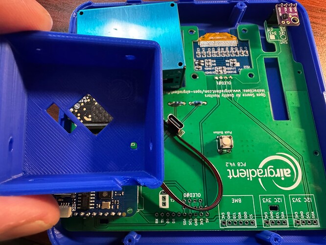
The STL file for the cable area of the DIY Pro 4.2 is wrong. The hole for the button is directly next to the USB-C port wheras the button on the PCB is actually much further away. I downloaded all other Pro STL files and they all had this problem. Does someone have the correct one?
If I remember right, aren’t there two buttons on the PCB? I haven’t printed that case, but I’m pretty sure the hole in my injection molded case is right next to the USB-C port as well and the only button I’ve ever needed to access was accessible through that hole.
There is no other button on the PCB. Here is a photo to illustrate my point, I am holding the cable area over the actual PCB:
Ok, I was thinking of the ONE board that has two switches.
You are trying to put the narrow rectangle over the USB port and not the larger one, right?
Yep the narrow rectangle fits the USB port perfectly but I cannot use this “cable area” because the other buttons sticks out and has no cutout. I could make my own but I am sure there must be a stl out there as this older design has been around for a few iterations.
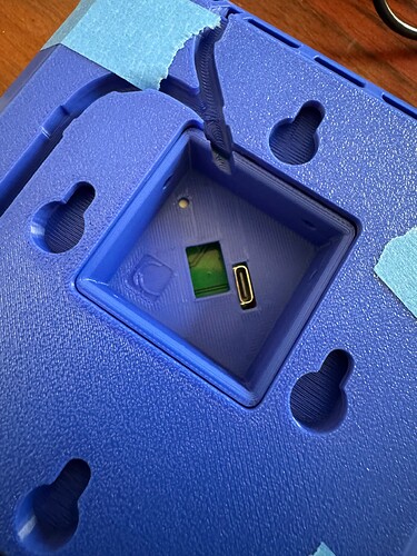
Oh I am stupid. I think the button is not supposed to fill out that square and is supposed to hide behind the whole so it can only be pressed by a pointy tool? Not sure why there would be that square hole but I think this is as intended:
Some models have some test pads that are accessible through the more square hole, although your board doesn’t appear to have it

