I2C investigation of Airgradient PCBs

I, too, was a bit surprised to see the 2 layer board with narrow power and ground traces, but I still think at these speeds and edge rates, you will not encounter issues due to SI or transmission line effects. DC IR drop for power was an initial concern, but the devices are drawing so little current (microamps to single digit milliamps), it really doesn’t even come into play.

It’s not DC resistance I’m concerned about - it’s the net impedance (and that is both the power and associated return (aka “ground”).
Most sensors average draw is very low with with peaks during the sensor measurement (e.g. S8 avg: 30mA, pk: 300mA), therefore the transient response, and hence the power net impedance is important. Thicker traces don’t make a meaningful difference there.

I rarely use I2C, but based on my measurements of 700ns risetime, that would only be sufficient for 100kHz (slow) I2C comms and would be marginal if a faster comms rate was used (e.g. more sensors, or some SW change down the line).

Okay. I’m going to need more data. My cheapy Rigol scope is coming in a few days, so if you would…

If you really want to prove that the power supply ripple is caused by PDN impedance, then you’ll have to do a proper PDN measurement. I don’t own a VNA and frankly, it seems like overkill. You should also measure the falling edge rate of the sensors. My guess is you’ll find the significant components of that edge won’t line up with very high impedance on the PDN plot.

I agree that voltage ripple is a potential problem, but it’s likely caused by something else on the rail.

First of all, it looks like you’re running at 400kHz, which is not default and obviously a stronger pull up will be required to trade off power for more speed. But it looks like many D1 minis already have severely undersized LDOs, so if we’re hitting a regulator current limit, this is just going to exasperate the situation. You’ll need to hit 300 nanoseconds. What’s the benefit of running I2C faster for air quality sensors? I see no advantages, so I’m curious.

And then the spikes on the rail look like they are spaced at 333.33 kHz, which is a clear sign that it is not caused by the device’s on the I2C bus switching. Assuming the measurement is good, it should be coming from the D1 mini itself probably. Did you measure the power at the decoupling capacitors of the sensor module to see if those spikes are better? The inductance of the long header pins may take care of a lot of that.

And you have to be careful. The S8 and PMS sensors run in 5V. The only thing on 3.3V (aside from D1 mini itself) are the I2C sensors. Even the OLED is on the 5V rail with it’s own 3.3V LDO. And if you look at the datasheets of the SHT and TVOC sensors, the power draw is low and the only thing external switching is the I2C interface.

So I agree there might be a reason to “fix” the 3.3V rail spikes, but it’s not caused by the PCBs PDN. I think. Because again, I’m blind here. Just operating with the data I have and what you guys have measured.

Now that I think about it: one way to know is to insulate the D1’s 3.3V pin and simply power the 3.3V with a bench top supply and see.

And now that I think about it some more: just unplug the D1 mini and measure the 3.3V on the D1 mini itself.

Do that and then we can go from there.

Edit: I want to emphasize that I’m not disagreeing. I’m just cautioning that we restrain from drawing conclusions with incomplete data.

Oh. One other thing… @Hendrik noticed that he also sees ripple on 5V. Perhaps that is the source and it’s coupling through the LDO. These LDOs’ PSRR probably isn’t going to stop any of those spikes. Here’s the PSRR on the LDO that I suspect is on my D1 mini board (XC6219):

It starts falling at ~40 kHz and we get no data above 100kHz, but I suspect it’s very poor. Something to investigate. Get some scope shots.

Well thats a lot of information, mind you I’m not an electronics engineer but an enthusiast. I made these measurements so I can have a better understanding of what I’m looking at and how to diagnose it. And learning something on the way.

First of all, I have no i2c issues. Only misbehaving sensor probably because lack of stable power supply. But particulary that SGP30 has caused a lot of issues for multiple people in the past. It has it’s own ldo to go to 1.8v and level shifters for i2c.

I will try to find where the spikes come from, possibly from the 5v and those are caused then by the battery module because all test were run on battery. I will try a usb supply en bench supply next time. (When no i2c signals are sent, and thus sensors are idle, both 5v and 3.3v only have about 50mV ripple.)

And I will try to find what component(s) causes the biggest ripple. Possibly I can feed it its own power to isolate the issue.

On this page you can read that internal 10k pullups will be enabled when defining a pin for i2c.

If you really want to prove that the power supply ripple is caused by PDN impedance, then you’ll have to do a proper PDN measurement. I don’t own a VNA and frankly, it seems like overkill. You should also measure the falling edge rate of the sensors. My guess is you’ll find the significant components of that edge won’t line up with very high impedance on the PDN plot.

I have a couple of VNAs but I also don’t care (or have the time). The spikes I show on the 3.3V supply are a combination of the power net and the supply impedance and they are the physical reality that is there.

First of all, it looks like you’re running at 400kHz, which is not default and obviously a stronger pull up will be required to trade off power for more speed.

I’m running the default SW, so it is whatever it is.

Did you measure the power at the decoupling capacitors of the sensor module to see if those spikes are better? The inductance of the long header pins may take care of a lot of that.

I measured on both but no - the long header pins will typiucally make things worse as that is an undamped inductance in parallel with the capacitance - forms a weakly damped LC filter which will cause more Vpp ripple not less (see Linear Technology app notes where they warn that such a system will cause voltage spikes)

I don’t think that the PCB layout is the root cause of all problems, but my measurements show that there are elements to be concerned about: there is a lot of ground bounce, marginal rise time and supply noise on 3.3V and that these are partly due to the supply / ground net.

Following a pleasant conversation with AirGradient I am confident that these things will be taken into account in the future.

I was under the impression that 100kHz was the default speed based on @Hendrik 's measurements. If 400kHz is default, then my original concern about the rise time being too slow is valid. Although, I think we could just slow down the I2C bus.

True if the noise is caused by switching noise at the sensor, but if it’s just spikes to the left of the LC, then it’s just a low-pass.

Switching noise just doesn’t have any meaningful effect with such low-power and slow I/Os. With only one I/O switching at any given time, the noise is definitely not caused by the sensors. There could be other issues, but it’s not originating from the poor PDN and poor signal + return path. Not with these devices.

I can’t find the GitHub page with the source, but my SCL measurements above indicate somewhere in the order of 400kHz.

True if the noise is caused by switching noise at the sensor, but if it’s just spikes to the left of the LC, then it’s just a low-pass.

Switching noise just doesn’t have any meaningful effect with such low-power and slow I/Os. With only one I/O switching at any given time, the noise is definitely not caused by the sensors. There could be other issues, but it’s not originating from the poor PDN and poor signal + return path. Not with these devices.

“the noise is definitely not caused by the sensors”
You mean the noise spikes in my scope captures?

You have at least 0.1uH of loop inductance due to the IO and signal wires, shunted in parallel with some capacitance. If you hit that with digital comms (I2C) with an edge rate of about 1V/us then it’s going to excite a resonance in this undamped LC circuit (the power network) which would be the spikes you see in
the screen captures.

I have added some info to my 3.3V line measurement.

I see you’ve updated the info on the measurement. Yeah, I agree it’s I2C switching noise.

@ken830 @l4ur @Hendrik many thanks for looking into this issue.

Our hardware team is also currently looking into this. It seems to affect only very few people but still it is something we want to improve and we currently follow a two step process.

1st to make some minor improvements to the PCB, e.g. adding ground planes, and a few other components e.g. capacitors to improve overall stability.

2nd step is to reduce the dependency on the 3rd party modules, like the D1 mini or some of the sensor modules because we do not really have influence on the quality and exact specs these manufacturers use (e.g. voltage regulators, pull-ups etc). So we plan to put an ESP32 directly on the PCB and add the necessary circuits required ourselves. The ESP32 would then also allow us to have a more robust overall MCU. We do follow a similar approach with our new outdoor monitor that we currently develop the circuits and if that works out well we will apply the same approach here.

Once we have some specific suggestions on these improvements, I will post them here so that people interested can have a look and comment.

I think the one downside to moving away from the modules is that it might make the "DIY "and the “open design” aspect of it quite a bit less accessible to a larger percentage of the people. And makes it a bit more difficult for people to make quick/easy modifications to the design. I know the design will still be open and the software library will still be freely available and those aspects are a very big piece of the openness. Just a concern… perhaps there’s a way to balance it.

Yes I agree and one option could be to have the current PCB based on the D1 mini still available for people that want/need this accessibility (eg for educational projects) but offer the more advanced board for people that need more stability.

1 Like

Agree that would be a suitable solution. Divergent hardware, but retaining SW compatibility.

I completely agree on the concerns about moving away from the DIY aspect if you go to directly connected chips. That is what got me so excited when I first heard about it on Jeff Geerling’s video, was being able to add and modify my own hardware in a beginner friendly way, with the PCB being the one part I don’t know enough about to make myself.
So keeping some kind of balance with being compatible with our own components is very appealing

Okay. A few things to share. I was tired of being “blind” and I don’t use company resources for personal projects, so I decided to finally pick up a scope for the home. I’m on a limited budget, but was able to get a Rigol MSO5000 series scope with the full bandwidth unlocked. Spec’d at 350MHz, but likely a bit higher according to others with the same scope. I’ve got a 6GHz RF generator coming, so I can test the actual bandwidth of the front-end, but it shouldn’t matter in this case as it’s more than good enough for what we’re doing. For the probe, I have a Tektronix P6139A 500MHz High-Z 10X 8.0pF passive probe connected and properly compensated.

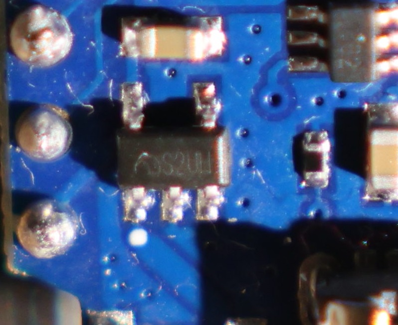
Last week, the LDO on my D1 Mini died (probably from my probing) and I had to wait for replacement clones from Amazon. It took about a week to get here. I suspect that LDO may be at the limit of its capability. From the marking and clues on https://github.com/bbqkees/Wemos-the-Clone-Wars/blob/master/README.md page, I think I may have a 150mA LDO. The replacement clones from Amazon seem to come with genuine MicrOne LDOs, but it’s not clear which one. The package marking shows the MicrOne logo and S2U??? Anyhow, I hope it’s got better than 150mA capability.

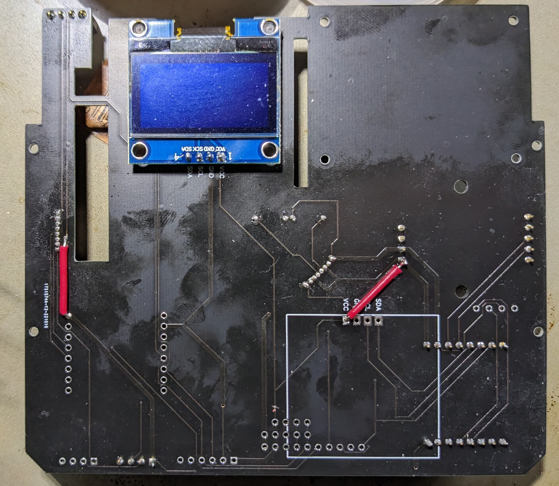
First of all, I’m not sure why I always thought the OLED on 5V, but apparently, I’m wrong. I don’t see why it’s not though, so I did some re-work on my v3.3 PCB:

For the SHT header, I cut the 5V trace and connected 3.3V. For the OLED, I cut the 3.3V trace and connected to 5V. Now the only thing on the 3.3V rail is the D1 Mini itself, the SHT and the SGP. The OLED, PMS, and S8 are all on 5V.

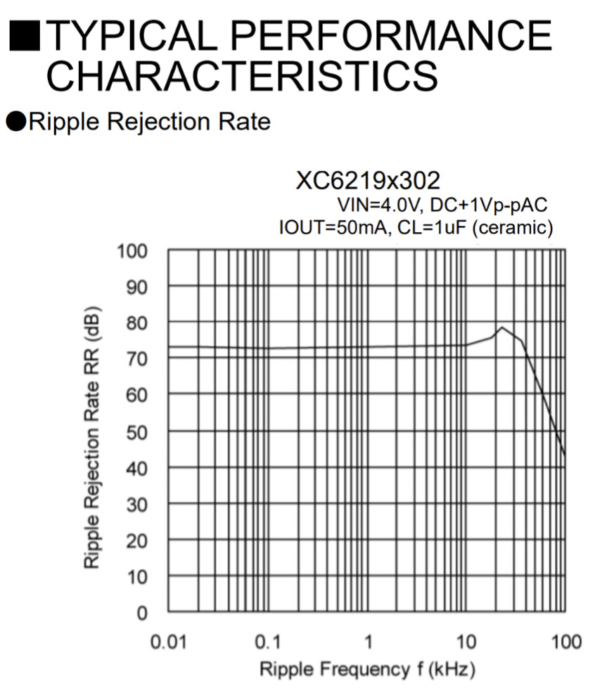
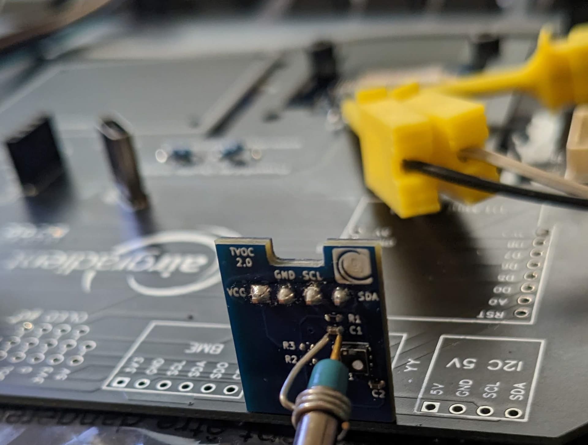
First, I measured 3.3V at the SGP module’s header pins, confirming about 200mVpp spikes aligning with I2C falling edges:

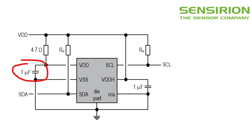
But proper supply measurements should be done at the decoupling capacitor with 20MHz bandwidth limit. The SGP module follows the recommended application circuit in the datasheet. So, I took measurements at the SGP41’s VDD decoupling capacitor (C1):

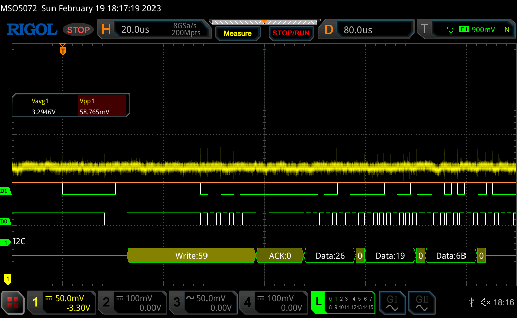
First, here’s the measurement without the BW limit:

Only about 60mVpp at the decoupling capacitor. I picked one of the bigger spikes and zoomed-in:

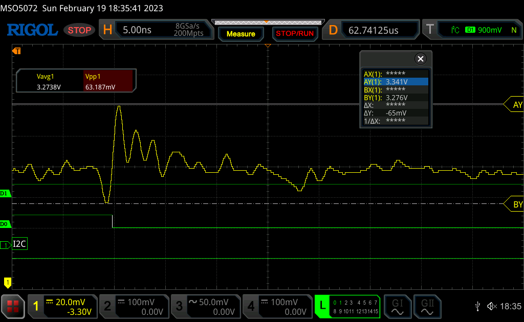
20mV/div is the limit of my scope (it goes into BW limit mode beyond that) and we can see the 8-bit quantization of the waveform. Looks to be roughly +40/-24 mV deviation. That’s only +1.2/-0.7% of 3.3V. But look at the rise time of that spike. It’s very high-frequency. The amplitude could be slightly greater as we might be nearing the bandwidth limits of my probe and scope. I was careful to maintain the full sampling rate of 8GSa/sec (0.125ns/sample period) to ensure we’re not aliasing here. To be sure, I turned on the dots display mode so you can see every sample:

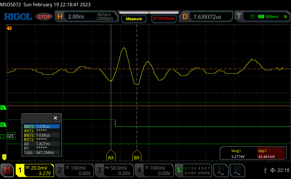
Looked at more of these spikes and I would say it’s roughly in the 500MHz ballpark:

So, I took measurements with a 20MHz bandwidth limit on the scope channel:

The ~60mVpp dropped to <18mVpp:

Zoomed in and I don’t see any effects aligned with falling edges:

Most of this is just the noise floor of my lower-end scope’s front-end. But either way, it’s looking pretty decent.

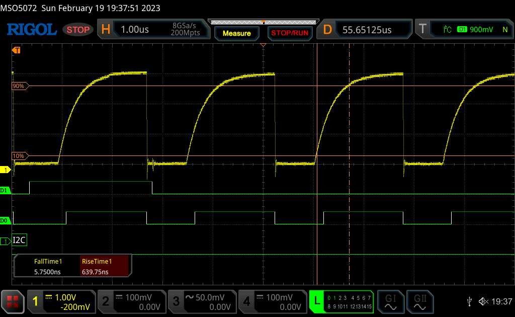
One concern was the rise times. Right now, my current configuration is unmodified so the SHT still has 10K pull-ups. And the OLED has 10K pull-ups. This gives me ~650ns rise times:

This is not meeting I2C fast mode requirement of 300ns. I think there’s no reason to run in fast mode. Reading a small number of sensors every few seconds and updating a 1-bit, low-res screen really doesn’t need anywhere near the data bandwidth of even standard mode I2C. Turns out u8g2 is running the bus at a default of 400kHz (fast mode). Back in 2018, someone asked (https://github.com/olikraus/u8g2/issues/705) why the bus speed was hard-coded and the u8g2 author was able to introduce a new function to set the bus clock rate: setBusClock(). So, I made a quick change to the Arduino sketch:

void setup()
{
Serial.begin(115200);
u8g2.setBusClock(100000);
u8g2.begin();

.
.
.
}

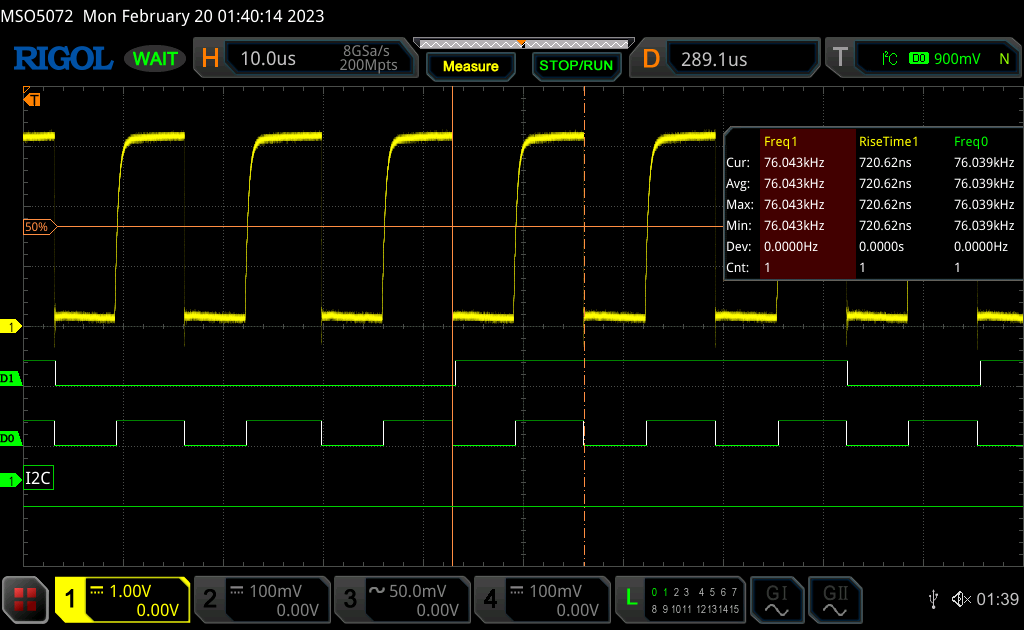
Strangely, this resulted in ~76kHz clocks rates:

Setting it to 133kHz seems to be spot-on for 100kHz clock rates:

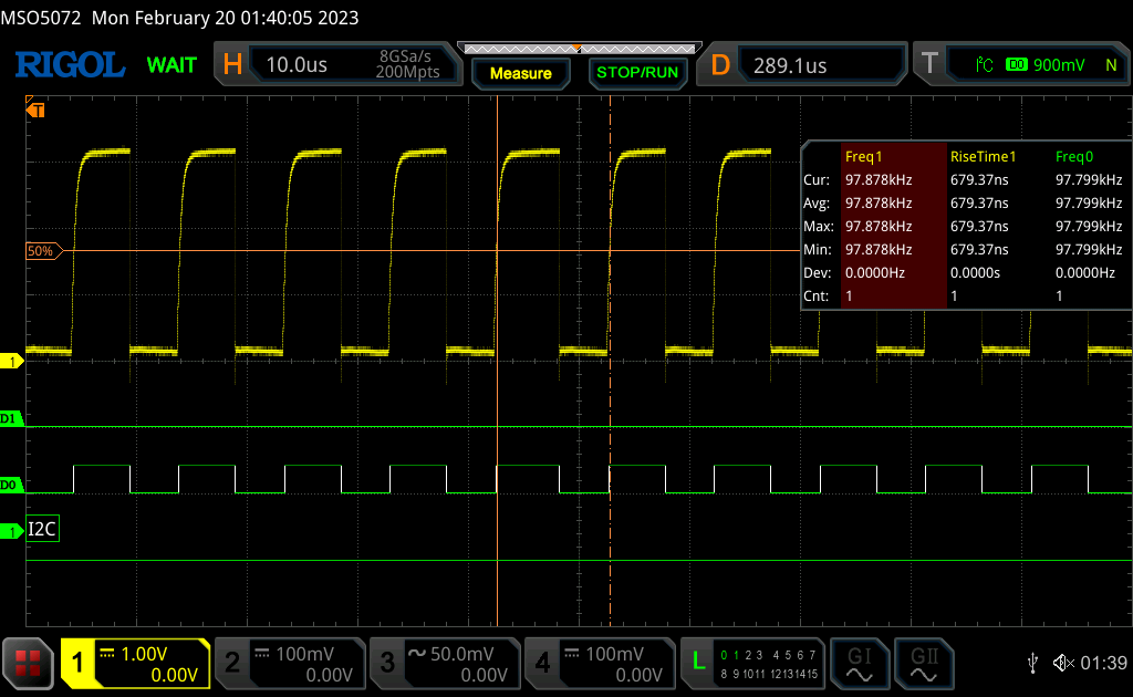
I then went ahead and tested a bunch of settings:

Set (kHz) Actual %
75 55.5 0.74
100 76 0.76
133 104 0.78
200 154.75 0.77
250 197.5 0.79
300 282 0.94
400 392 0.98

I know I2C clock speeds aren’t exact, but still seems strange to be so far off in the lower range – it’s not linear and there’s a major bend point around 300kHz. I created an issue on Github to inquire the reasoning behind this. For now, I have it set to 100kHz and let it run slower (~76kHz). Screen and all sensors work just fine. This thing is rock solid so far.

Here’s what AirGradient needs to do: release the original EDA files (schematic and PCB files) for the DIY products. The fact that up until somewhat recently the closest thing to a schematic available could have been drawn in Paint, makes me sad.

It looks like the PCB v3.7 schematic might have been made in EasyEDA. Either way, if the DIY version is intended to be truly open, just release the original EDA|ECAD files and let the community fix it. The existing Gerber files would have to be reverse engineered without the original files.

I’d keep them same physical design and component placement, but have the bottom layer of the PCB as a ground plane with only very short jumps from the top layer as needed. This is not a complicated board. Zero need for more than two layers. Then I’d add a footprints for SMT and THT capacitors (for DIY options) for each component as is good engineering practice. Oh, and release a real BOM. Is the PN for the USB-C connector even specified anywhere?

After all of this, then we could consider adding an extra LDO or something if there are power rail issues or the WeMos modules are using questionable regulators. I might also consider replacing the WeMos with a Raspberry Pi Pico W to avoid needing AliExpress to source a core component like the microcontroller, assuming there are real issues with the WeMos clones.

I’d be surprised if it wasn’t possible to just keep using the WeMos clones with some small workarounds, though.

We are currently transitioning from easyEDA to kiCad.

The kicad files have already been published in another thread but you can also download them from this temporary folder:

https://drive.google.com/file/d/1z6g0-oY6amFZzEOuNfQ8zrduPmo9SX5o/view?usp=share_link

We are a bit in a transitioning phase right now and the project documentation (incl. BOM) are not well structured and missing some pieces at the moment but I expect the whole structure to get much better over the coming weeks.

1 Like

@ken380, do you think that the ground plane under the ‘KEEP OUT’ area of the microcontroller will affect wifi reception?

Thank you for making the files available and for the thoughtful reply. I apologize for the excessive snark in my previous message.

Yes this somehow slipped through our review and needs to be corrected.

1 Like

@scottsm : Good point. Looks like it will be corrected. I’ve never worked with wireless devices before and have no special skills in wireless, so it’s not something I looked for instinctively.

@Achim_AirGradient : also it looks like “SDL” should be “SDA” in the silkscreen layer.

1 Like