I2C investigation of Airgradient PCBs

Having some problems with getting the SHT3x to work in the socket, works in 5V the top socket. I have the TVOC connected to 3.3V I2C.
Looking at the Gerbers, the whole PCB is only 2 layers, no ground plane - In my 25 years of designing HW, I’ve always used ground planes, especially with digital comms.

Is this the reason that people are having problems with intermittent comms issues?!
Looking at the routing of the SDA/SCL on the bottom 5V I2C - the ground net follows a completely different route! Therefore the impedance on the SCLK and SDA would be large and probably cause rise/falltime issues that are highly dependent on termination values (certain values may “just-about” work depending on what else is connected to that spaghetti bus)

For the price of the Pro kit, I think that a 4 layer PCB should be expected (probably required for meeting CE requirements if anyone was considering re-selling these!)
Edit - this could probably even have been routed on 2 layers, with solid ground plane and using a bunch of crossover resistors / wires

Around two weeks ago we started shipping the kits with an upgraded board (pcb version 3.7) that has now the i2c bus completely on the same voltage level as the mix of 5v and 3.3v was not compliant and likely the cause of issues some people had.

If you received the old board please contact our support and we will send you the new version free of charge.

We tested new board quite extensively and I did not experience these issues anymore on it.

I will feed back your comments on the ground plate to our hardware engineer for the next iteration. It was something we looked at before but I am not sure why it was not (yet) implemented.

This being a 2-layer board with no return current path is extremely unlikely to be the cause of any I²C stability issues here. The concern is valid for “high speed” signals. Of course, “high speed” is based on the signal protocol’s UI and the edge rate. I²C being operated at 100-800kHz means that our UI is well over 1 microsecond at worst. Even being generous with saying the trace length of the AirGradient PCB is 12 inches here, that’s still plenty of time (several orders of magnitude more) for any potential reflections to settle. That’s good because the rise-time of the signal is a bit harder to pin-point. Because I²C is is a shared open-collector/drain, the rise time is fully dependent on the pull-up resistor we choose and the bus capacitance. The resistor here is 10Kohm (or 5Kohm if we accidentally or purposely have a double-set of resistors to the same rail), which is pretty weak. For the bus capacitance, it’s really an unknown… but somewhere in the around 100 picofarad range is probably reasonable. All that to say the rise time of the I²C signals are going to be well slow enough to not be of any concern here. Actually, the concern might be the rise time is too slow if bus capacitance is too high and if you run the I²C bus faster than 400kHz. I don’t have an oscilloscope at home, but if someone does, it would be nice to measure rise times and we can reverse calculate the bus capacitance. Maybe I finally pick one up.

The more likely explanation for intermittent i2c is because there is likely two sets of pull-ups (one set on the SHT to 5V (PCB v3.3 and below) and one set on the OLED board to its 3V LDO rail). Removing the SHT resistors is probably enough to make it reliable, although I haven’t gotten around to doing that yet. The SHT on 5V means that pull-ups to 3.3V is not fully meeting VIH min requirements, so it really needs to be on the 3.3V rail. I’m planning to cut a trace and rework it with a wire to demonstrate it is possible.

True - but it’s not going to help - especially as the fast mode I2C narrows the acceptable range of resistor pull-ups values - combined with a variable number of bus units lowers the margins for successful comms - even if all the devices fully meet the I2C specifications.

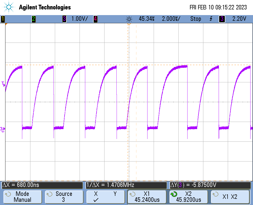
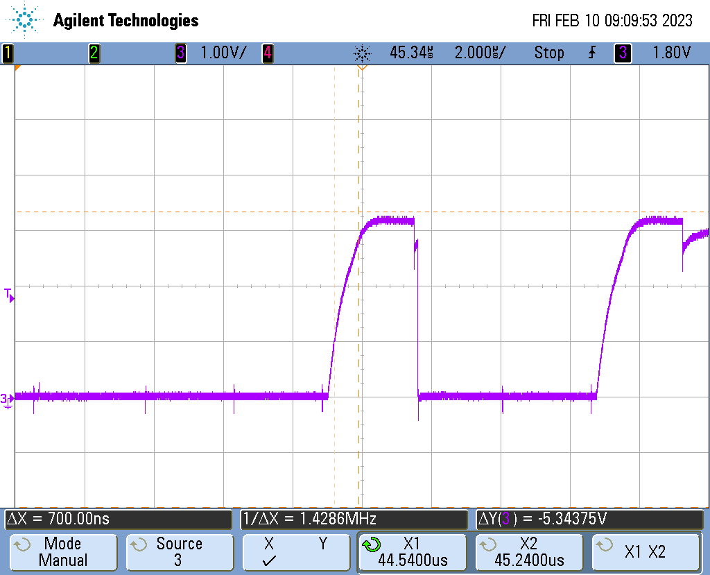
Rise time: "the maximum rise time for standard mode and fast mode is 1,000 ns and 300 ns, respectively. "
This App note mentions quite a few issues, that again can be related to sub-optimal layout and subsequent margins.

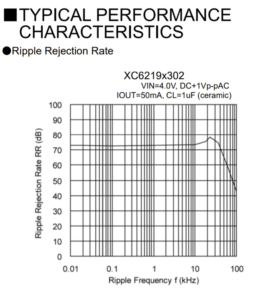
In any case - for the modules themselves, a good voltage source would be nice to avoid PSRR from cross-modulating on the measurements (unless real care has been taken in the decoupling choices).

The 5V stuff should probably have had a level translator on the I2C comms (yes - it “can” work but again the margins become very small).

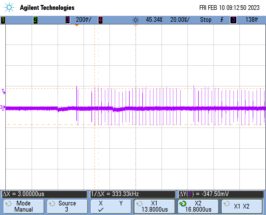
I also think that running SCLK lines far from ground is a bad neighbourly thing to do w.r.t. EMI / EMC, so this probably could not ever be made CE compliant. In addition this may be another source of intermittent problems as the traces can pick up EM signals, and rectify them, causing glitches. By running them near a ground plane the loop areas are reducing, inducing less current through the trace and thus less voltage.

Now, can the AirGradient PRO work? Sure, it can - but unless I see a design document that showed someone had put some engineering thought into it I would not have let it go through design review.

Even with my own little projects, I write down some sentences and perform some calculations (especially with mixed 3.3V /5V systems).

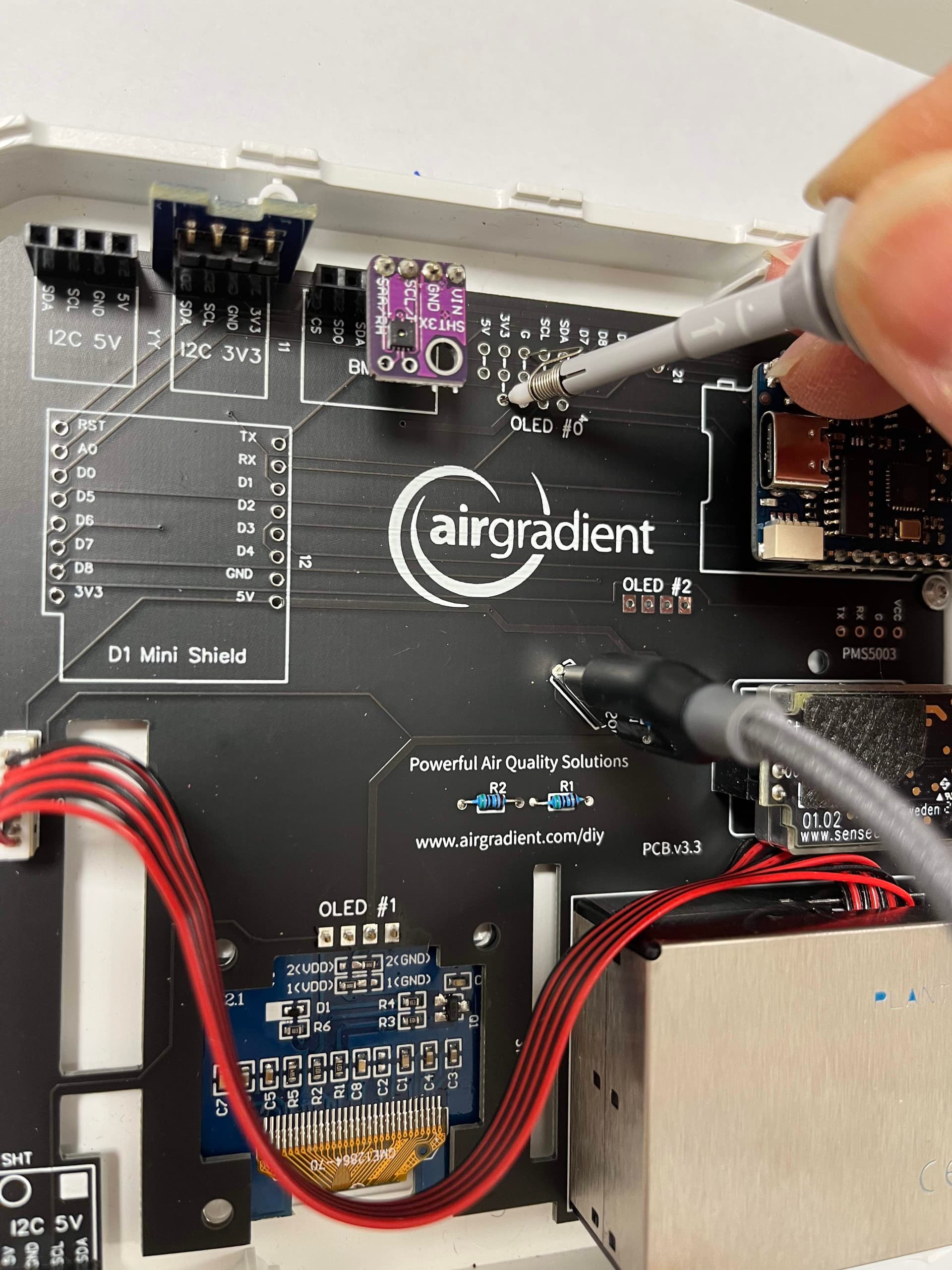
My SHT3x (PU removed) works in the top left 5V socket, but not in the bottom 5V socket…

In any caes both my digital scopes are at work - and TBH I’m not that interested to debug a design that I think is fundamentally flawed.

Due to postage cost and import taxes I bought 3 - Pro kits in the belief it would save me the time of doing design myself (especially the SW framework).

Therefore I’m doing a quick PCB myself now, with a few additional 3.3V headers, a well-decoupled 3.3V rail with its own 5V - 3.3V regulator with good, broadband PSRR (who knows what the USB power supply spits out) and external caps at each I2C node, so that I’m not reliant on the lowest bidder X5R or worse caps fitted on most boards. This way I can re-use the SW, modules and the nice case.

I’m analog and systems designer, but I’ve done my share of high speed digital and PCB design.

All of this of course in my own opinion and I’m supportive of the aims of this project, so I’m keen to get the ones that I invested in working (also so that I can send one to my older asthmatic family member - I would be interested to see if their symptoms are correlated to the PM2.5 and CO2 levels)

Will follow this. I have no background in any of this but just an enthusiast with a reasonable oscilloscope since a few weeks. I’ll try to do some measurements next week to let us determine where the actual i2c issues are coming from.

Maybe we can give some reference what the amount of pullups should be when x amount of sensors is used. It would help my setup and other with the older PCB. Or even improve the new PCB. @l4ur Can you share youre design when its working?

For the price given I didn’t expect a well engineered board but good enough for DIY. Otherwise you shouldn’t even look at this and buy the “professional” systems at triple the price.

I, too, was a bit surprised to see the 2 layer board with narrow power and ground traces, but I still think at these speeds and edge rates, you will not encounter issues due to SI or transmission line effects. DC IR drop for power was an initial concern, but the devices are drawing so little current (microamps to single digit milliamps), it really doesn’t even come into play. Sure… in extremely noisy environment, you could probably induce something on the traces, but I don’t know how exactly how likely that is. Only thing I would be concerned about is the possibility of slow rise times of the I²C bus due to weaker pull-ups, but will need a quick look on a scope to determine that.

When I first received the kit ~ 2-3 weeks ago, I immediately noticed I²C instability and reboot issues, but dug through the design and all the datasheets and was able to determine the issues stemmed from the dual sets of pull-ups and the mix of 5V and 3.3V incompatibility. Another week of work and some collaboration with the contributors of the ESP8266 Arduino and SoftwareSerial libraries, and I was able to root cause the frequent reboots as a recent code change to the serial port library – this is still on-going, but we have a workaround for now.

I haven’t looked into the serial-port connected sensors (PM & CO₂ yet), so I may find something there when I get around to understanding the sensors.

That said, it’s not a bad idea to re-design the board with dedicated power and ground planes. I have similar plans to do so and to add some features I have in mind.

A lot of people have strongly-held opinions when it comes to PCB design and SI/PI and most of the industry operates with rules of thumb, but in reality, these components operating at these speeds drawing these levels of power really is a very forgiving environment.

I just talked to our hardware team. The PCB that we currently ship (v. 3.7) already has larger traces and we are also doing a review of the board for further improvements, e.g. ground plane and additional components (e.g. capacitors) that could increase stability.

As soon as I have a list of improvements, I will post it here for comments.

Unfortunately with the pull up resistors we do not have too much control as the OLED display and the SHT are 3rd party modules.

Some preliminary results. I did testing with esphome and the latest version of airgradient arduino code. The results for i2c rise and fall times are about the same. As expected. So I keep testing with esphome where I can easily disable a sensor without removing and changing the pullup resistance.

i2c is running at 100khz or standard mode which allows up to 1000ns rise time. (Only pullups to 3.3v, no 5v is used for any of the sensors.) For the most combinations of sensors its below 600ns on both scl and sda. The fall times are much, much lower because of the sensors sink capability.

I also looked at the 3.3v rail. While commands are sent by i2c bus the voltage fluctuates, as I would expect. I measured up to 1.1vpk/pk. But that seems to me a bit much so I added some caps and reduced it to 0.8v.
Also the same voltage drops are seen on 5v supply so maybe its better to add some capacitors there?. Please let me know what I should expect cause maybe it isn’t that bad as I presume.

The problem that I still have is that the SGP30 isn’t always setup by esphome. They have a routine to check if the sensor is present and working otherwise it will not be initialized. Many times it doesn’t work but it looks like with a more stable 3.3v supply I have more luck initializing and a working sensor. This doesnt mean the SGP30 isn’t working but it will not pass esphome tests and you are not able to get any data.(Other problem is infrequent crashing but there are other topics on this)

So far I don’t see any major i2c problem. It does what it should do and signals are looking the same wherever I measure it on the board. So I agree with @ken830 that even if the pcb isn’t as optimal as it could be it still works most of the time. Though the right amount of pullup resistance should always be calculated/added. And this is a work in progress to see what the limits are on my old 3.1 pcb.

At a later moment I will check what my resistance is because a lot of components play part in this, even the esp itself. ESPhome adds the pullup internally in its i2c routine, I’m not sure how it works in the library for arduino.

I will add that the 3.3v always comes from the D1 or equivalent controller and not every unit is as capable as a wemos is. That ldo is rated for 500mA. More information about this issue here https://www.reddit.com/r/esp8266/comments/9iizx4/warning_clone_wemos_d1_minis_with_only_150ma_33v/

I checked my D1 mini which came with the airgradient pro package is not a genuine wemos but the ldo has printed DE=A1D on it and that is rated for 300mA by some sources. I did not calculate what the total current is with my sensors yet so I can’t if some issue arrises there.

@Hendrik : The schematics for on the Wemos site calls for a ME6211, which is a 500mA LDO, but I suspect many of the D1 Mini boards in the wild have much less capable LDOs. On mine, I can see “LB2K” marking, which seems to likely be an XC6219, which is 300mA part. Although, I would say that the 3.3V load (outside of the D1 Mini itself) is really minimal.

Still, I would suspect something else is wrong if you are seeing 1.1Vp-p ripple on the 3.3V rail. That’s very concerning.

I haven’t dug into the MCU side of things… You’re saying there are internal pull-ups enabled on the GPIOs used for the I2C bus? We would need to sort that out.

How many pull-ups do you have on your board in total? Remember there is also an LDO (5V => 3.3V) on the OLED PCB that has 10K I2C pull-ups attached.

I have an oscilloscope coming so I could probably make some observations on my end as well.

EDIT: Looks like my LDO might be the XC6219B, which is only 150mA.

A fee comments from my side.

We currently use a knock off D1 mini because we had received faulty originals where the WiFi was not working reliably and interestingly the non original ones were running much better. I wrote about this in our blog.

Medium term we want to move away from the D1 modules and directly put an ESP32 C3 onto the board. Then have control on which exact voltage regulator etc we use.

Then also add smd resistors and caps as required.

So basically reducing the dependency on 3rd party modules where we don’t know exactly what components (voltage regulators, pull ups etc) using.

1 Like

Here are my measurements
Power was from a Anker Batter pack with high quality USB C cable.

PMK scope probe is compensated (important for square wave signals). About 15pF tip capacitance, 350MHz BW. Scope is an Agilent with 1GHz BW.

Note how I perform the grounding (not with the standard ground leads).

Unit has SHT3X (PU removed) and TVOC sensor.
I have put the SHT3X in a 3V3 socket.
Note the noise on the 3.3V line (350mVpp) due to comms - those can effect the measurements on modules that use 3.3V directly for reference, depending on Vref PSRR.

Note the undershoot (500mV) on 3V3 - that is real undershoot, not a measurement artifact.

Rise time is about 700ns, not great (and again, I’m on a fully 3.3V system now).
SCL, SDA and 3V3 lines (latter is AC coupled measurement to show the I2C comms noise)

SCL

SDA

3.3V line, measure relative to the pin labelled G. AC coupled scope probe.
The spikes are ~2.6us (~380kHz) and in bursts - hence likely to be the I2C comms, not the supply to the AG Pro

I, too, was a bit surprised to see the 2 layer board with narrow power and ground traces, but I still think at these speeds and edge rates, you will not encounter issues due to SI or transmission line effects. DC IR drop for power was an initial concern, but the devices are drawing so little current (microamps to single digit milliamps), it really doesn’t even come into play.

It’s not DC resistance I’m concerned about - it’s the net impedance (and that is both the power and associated return (aka “ground”).
Most sensors average draw is very low with with peaks during the sensor measurement (e.g. S8 avg: 30mA, pk: 300mA), therefore the transient response, and hence the power net impedance is important. Thicker traces don’t make a meaningful difference there.

I rarely use I2C, but based on my measurements of 700ns risetime, that would only be sufficient for 100kHz (slow) I2C comms and would be marginal if a faster comms rate was used (e.g. more sensors, or some SW change down the line).

Okay. I’m going to need more data. My cheapy Rigol scope is coming in a few days, so if you would…

If you really want to prove that the power supply ripple is caused by PDN impedance, then you’ll have to do a proper PDN measurement. I don’t own a VNA and frankly, it seems like overkill. You should also measure the falling edge rate of the sensors. My guess is you’ll find the significant components of that edge won’t line up with very high impedance on the PDN plot.

I agree that voltage ripple is a potential problem, but it’s likely caused by something else on the rail.

First of all, it looks like you’re running at 400kHz, which is not default and obviously a stronger pull up will be required to trade off power for more speed. But it looks like many D1 minis already have severely undersized LDOs, so if we’re hitting a regulator current limit, this is just going to exasperate the situation. You’ll need to hit 300 nanoseconds. What’s the benefit of running I2C faster for air quality sensors? I see no advantages, so I’m curious.

And then the spikes on the rail look like they are spaced at 333.33 kHz, which is a clear sign that it is not caused by the device’s on the I2C bus switching. Assuming the measurement is good, it should be coming from the D1 mini itself probably. Did you measure the power at the decoupling capacitors of the sensor module to see if those spikes are better? The inductance of the long header pins may take care of a lot of that.

And you have to be careful. The S8 and PMS sensors run in 5V. The only thing on 3.3V (aside from D1 mini itself) are the I2C sensors. Even the OLED is on the 5V rail with it’s own 3.3V LDO. And if you look at the datasheets of the SHT and TVOC sensors, the power draw is low and the only thing external switching is the I2C interface.

So I agree there might be a reason to “fix” the 3.3V rail spikes, but it’s not caused by the PCBs PDN. I think. Because again, I’m blind here. Just operating with the data I have and what you guys have measured.

Now that I think about it: one way to know is to insulate the D1’s 3.3V pin and simply power the 3.3V with a bench top supply and see.

And now that I think about it some more: just unplug the D1 mini and measure the 3.3V on the D1 mini itself.

Do that and then we can go from there.

Edit: I want to emphasize that I’m not disagreeing. I’m just cautioning that we restrain from drawing conclusions with incomplete data.

Oh. One other thing… @Hendrik noticed that he also sees ripple on 5V. Perhaps that is the source and it’s coupling through the LDO. These LDOs’ PSRR probably isn’t going to stop any of those spikes. Here’s the PSRR on the LDO that I suspect is on my D1 mini board (XC6219):

It starts falling at ~40 kHz and we get no data above 100kHz, but I suspect it’s very poor. Something to investigate. Get some scope shots.

Well thats a lot of information, mind you I’m not an electronics engineer but an enthusiast. I made these measurements so I can have a better understanding of what I’m looking at and how to diagnose it. And learning something on the way.

First of all, I have no i2c issues. Only misbehaving sensor probably because lack of stable power supply. But particulary that SGP30 has caused a lot of issues for multiple people in the past. It has it’s own ldo to go to 1.8v and level shifters for i2c.

I will try to find where the spikes come from, possibly from the 5v and those are caused then by the battery module because all test were run on battery. I will try a usb supply en bench supply next time. (When no i2c signals are sent, and thus sensors are idle, both 5v and 3.3v only have about 50mV ripple.)

And I will try to find what component(s) causes the biggest ripple. Possibly I can feed it its own power to isolate the issue.

On this page you can read that internal 10k pullups will be enabled when defining a pin for i2c.

If you really want to prove that the power supply ripple is caused by PDN impedance, then you’ll have to do a proper PDN measurement. I don’t own a VNA and frankly, it seems like overkill. You should also measure the falling edge rate of the sensors. My guess is you’ll find the significant components of that edge won’t line up with very high impedance on the PDN plot.

I have a couple of VNAs but I also don’t care (or have the time). The spikes I show on the 3.3V supply are a combination of the power net and the supply impedance and they are the physical reality that is there.

First of all, it looks like you’re running at 400kHz, which is not default and obviously a stronger pull up will be required to trade off power for more speed.

I’m running the default SW, so it is whatever it is.

Did you measure the power at the decoupling capacitors of the sensor module to see if those spikes are better? The inductance of the long header pins may take care of a lot of that.

I measured on both but no - the long header pins will typiucally make things worse as that is an undamped inductance in parallel with the capacitance - forms a weakly damped LC filter which will cause more Vpp ripple not less (see Linear Technology app notes where they warn that such a system will cause voltage spikes)

I don’t think that the PCB layout is the root cause of all problems, but my measurements show that there are elements to be concerned about: there is a lot of ground bounce, marginal rise time and supply noise on 3.3V and that these are partly due to the supply / ground net.

Following a pleasant conversation with AirGradient I am confident that these things will be taken into account in the future.